Processing Challenges of Granite Bases for Semiconductor Equipment (The industry’s strictest and most authenticpain points, directly applicable for process handover and customer communication)
Granite bases for semiconductor equipment (wafer inspection, optical alignment, vacuum platforms, lithography auxiliary bases, precision motioatforms) are not on the same level as ordinary machine tool bases. The core challenges are concentrated in seven major areas: material purity, ultra-high precision, cleanliness and notism, stress stability, complex irregular structures, surface micro-quality, and assembly consistency. The following explains each point thoroughly, covering all practical pain points from the factory.
I. InhereDifficulties in Stone Selection (Highest threshold for semiconductors)
Must be highly dense, free of impurities, and free of large crystal grains.
Ordinary Jinan BlaIndian stone is unacceptable; special-grade material must be selected with ultra-fine grains, uniform blackness, no yellow lines, no white veins, no pores, and no hidden ks. Tiny impurities will later shed powder and contaminate wafers.
Strictly non-magnetic
Cannot contain ferromagnetic minerals; otherwise, it will interfere with optical inspection ic alignment, causing equipment precision drift.
Coeficiente de dilatación térmica extremadamente bajo
At a temperature change of 1°C, deformation must be on the micron level; ordinary granite is directlliminated.
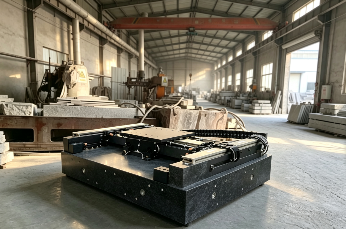
II. Extremely High Precision Grade, Tolerances reaching Micron and Sub-micron Levels
Flatness, parallelism, and perpendicularity requirde 000; flatness can reach within 1μm, far exceeding the conventional Grade 00.
Hole spacing, locating pin holes, and threaded bushing position tolernces are ±0.01mm to ±0.005mm.
Multiple datum surfaces, multiple inclined surfaces, and irregular guide surfaces must all meet precision standards simultaneously, increasing difficulty exponenially.
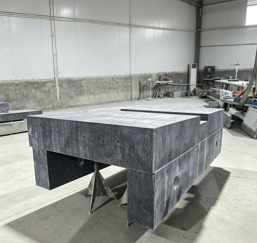
III. Complex Irregular Structures, Processing Prone to Chipping and Hidden Cracks
Common structures of semiconductor bases:
Large-area hollowing for weight reduction, thin-walled strues, deep grooves, and irregular steps
Dense counterbores, vacuum suction grooves, wiring grooves, and irregular bosses
Difficulties:
Many internal right anglese is brittle, and even tiny chipping is not allowed as it will shed dust and contaminate wafers.
Thin-walled hollow parts have high vibration during processing, easilng invisible micro-cracks and hidden cracks that slowly expand during later use.
Vacuum grooves are narrow and deep with poor chip evacuation; tool wear is fast, and surface is difficult to control.
IV. Greatest Difficulty in Stress Control, Stability Requirement of No Deformation for Ten Years
Semiconductor equipment operates in constant temperature workshops year-round; even slight deformatrectly leads to alignment failure and yield reduction.
Bases have uneven thickness and many hollow sections, resulting in extremely complex internal stresses.
Conventional natural aging is insufficient; constant temperature theging ultra-long ambient temperature curing is required, taking 7 to 15 days.
No further aging is allowed after grinding; any rework results in direct scrapp.
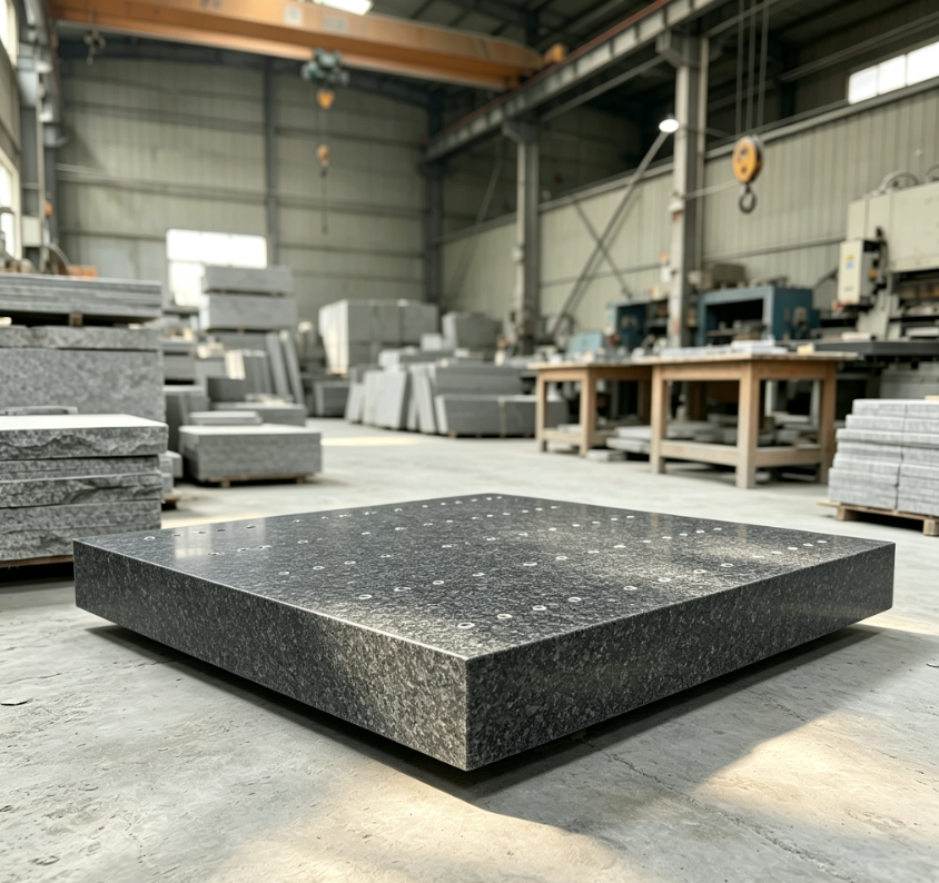
V. Insane Requirements for Surface Micro-Quality and Cleanliness
Surface roughness Ra < 0.2μm, with no scratches, tool marks, or residual grinding partis.
No oil seepage, water stains, dust, or stone powder residue is allowed; otherwise, it will contaminate the semiconductor cleanroom.
Grinding must be dust-free wet fne grinding; ordinary mechanical grinding cannot meet cleanliness standards.
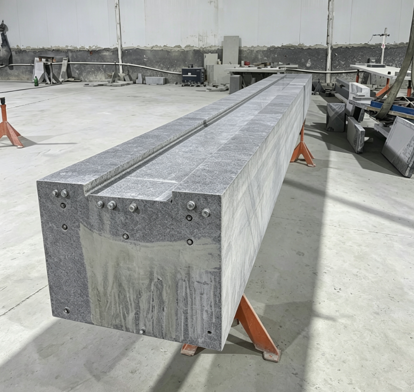
VI. Difficulties in Processing Embedded Parts, Vacuum Interfaces, and Sealing Structures
Verticality and coaxiality of staeel threaded bushings, vacuum connectors, and locating pin bushings are extremely high; gluing must be straight and secure.
Inner walls of vacuum grooves must be smooth ad burr-free; otherwise, there will be leakage and insufficient suction.
Sealing surfaces require extremely high flatness and must have no slight undulations.
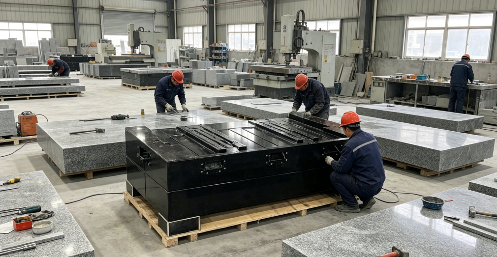
VII. Stringent Requirements for Processing Environment, Temperature Control, and Tooling
Processing must be conducted in a constant-temperature workop (20±2°C), as temperature fluctuations directly lead to processing errors.
Tooling must achieve precise positioning; clamping irregular parts is difficult and prone to tool vibration.
Tools must be ultra-fine giamond tools, with extremely slow cutting parameters, resulting in long processing cycles and high costs.
VIII. Post-Processing Protection and Contamination Control
Ordinary protectants cane used; food-grade, dust-free, non-volatile granite-specific protection must be applied to avoid contaminating the chip with volatiles.
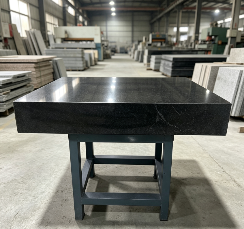
Edge chamfers must be uniform and smoree of sharp corners, to prevent chipping.
Summary of Core Challenges
High-purity non-magnetic stone sub-micron precision complex hollow thin walls zero chippiand micro-cracking long-term stress stability ultra-clean surface constitute the highest barrier for semiconductor granite bases.