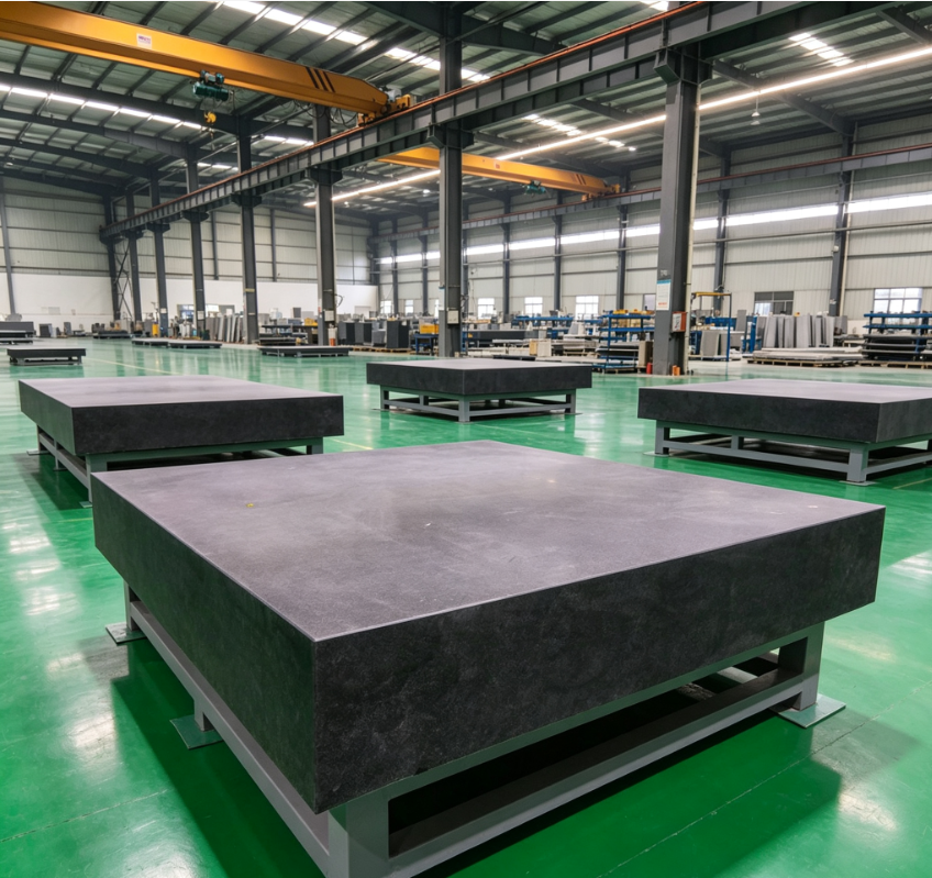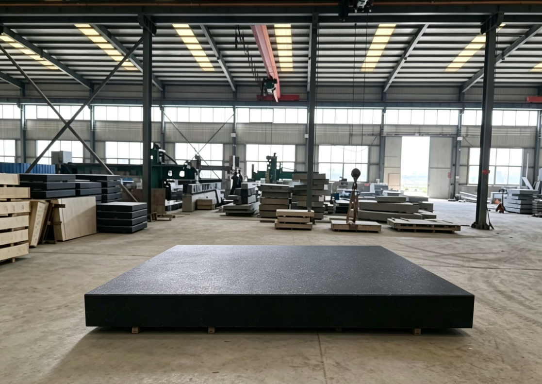
Specific application scenarios of granite countertops (commonly referred to as marble countertops in the industry) in the full process of chip manufacturing
Note: The “marble countertops” mentioned in the semiconductor industry are all black precision granite. Ordinary calcium carbonate marble is corrosion-resistant and has poor precision, so it is not used in chip production lines; all implementation scenarios are categorized into five major sectors: front-end manufacturing, wafer processing, metrology and inspection, back-end packaging, and laboratory metrology:
I. Core equipment for front-end lithography (the highest demand scenario for nanometer processes)
EUV/DUV/ArF lithography machine main chassis, wafer stage / mask stage base
Carries the air-bearing XY stepping scanning platform and laser interferometry system; granite isolates micro-vibrations from cleanroom fans and forklifts, and its extremely low thermal expansion offsets equipment heat deformation, enabling sub-nanometer alignment exposure for 3nm/5nm advanced processes, making it a core reference component of the lithography machine.
Electron beam lithography (EBL) and laser direct writing equipment countertops
Electron beams are extremely sensitive to vibration and static electricity; granite is insulating, does not scatter electron beams, and provides strong damping to suppress spindle vibration, used for mask writing and micro-nano chip patterning with line widths down to 10nm.
Coater and developer positioning platforms
Stably carries wafer carriers, preventing countertop deformation that causes uneven photoresist thickness and pattern offset, thereby improving exposure yield.
II. Wafer processing equipment countertops (wafer dicing / thin film / etching)
Wafer dicing machines, laser cutters, and ultra-thin wafer grinding machine bases
With spindle speeds of 30,000–60,000 rpm, cutting vibrations are extremely strong; granite quickly absorbs impacts, ensuring flat adsorption of 4/6/8/12-inch silicon wafers, significantly reducing wafer chipping and dicing offset defects, suitable for silicon, silicon carbide, and sapphire wafer processing.
CMP (Chemical Mechanical Polishing) equipment load platform
Under high polishing pressure and continuous friction, granite’s high rigidity ensures no long-term deformation, guaranteeing global wafer flatness and avoiding local over-polishing or under-polishing.
Internal precision motion bases for etching, PVD/CVD thin film deposition equipment
Corrosion-resistant to acids and bases, with no metal dust precipitation, suitable for vacuum chamber environments, serving as the displacement reference for wafer carriers to prevent uneven thin film deposition thickness.
III. Wafer metrology & defect inspection equipment (all scenarios of quality control)
Optical inspection (AOI) and electron beam inspection (EBI) defect detection bases
Carries high-definition optical lenses and high-speed displacement slides; tiny vibrations can cause image blur and defect misjudgment, so granite provides a stable imaging reference, essential for online high-volume wafer defect screening.
Film thickness testers and 3D profilometer platforms
For nanometer-scale thickness and height measurement, relying on the constant planar reference of granite to eliminate measurement errors caused by temperature drift.
Wafer sheet resistance / four-point probe electrical testing equipment beds
Scans the entire wafer to test resistivity uniformity; granite suppresses vibration, ensuring stable probe pressure and high repeatability of measurement data.
Mask calibration tables and laser interferometer reference platforms
Used for optical path and grating scale calibration, maintaining a micron-level planar reference over the long term to reduce the frequency of equipment recalibration.
Semiconductor-specific Coordinate Measuring Machine (CMM) worktables
Detects geometric tolerances of silicon wafers, carriers, fixtures, and lithography masks, matching the granite platforms supplied with the complete Hexagon CMM equipment set in your document.
IV. Back-end Advanced Packaging Equipment Worktops (Chip Bonding / Die Attach)
Die Attach Machine and Fully Automatic Wire Bonder Bases
Chip micro-solder point positioning accuracy within ±1μm; granite vibration isolation prevents wire bonding offset, reducing defect rate from 0.3% to 0.01%, suitable for power chip and Mini/Micro LED packaging.
Flip Chip Bonder and 2.5D/3D Packaging Alignment Platforms
Low thermal deformation under high-temperature bonding conditions, ensuring micron-level precise alignment between chips and substrates.
Packaging Finished Product Visual Inspection and X-Ray Inspection Load Platforms
Stable visual inspection reference for mass-produced packaged components, preventing false soldering, voids, and missed inspections caused by vibration.
V. Ultra-Precision Air Bearing Motion Platform Universal Bases (Compatible with all high-precision semiconductor equipment)
Core semiconductor precision motion units all adopt granite air bearing bases:
Air bearing linear guide and rotary platform installation reference;
Embedded copper-inlay guide strips, stainless steel threaded sleeves, and vacuum suction grooves;
Maintains a constant air film gap, ensuring nanometer-level repeatability for linear motors and grating scales; lithography machines, dicing machines, and inspection machines are all standardly equipped with this structural component.
VI. Laboratory / R&D Metrology Application Scenarios
Atomic Force Microscope (AFM) and Scanning Tunneling Microscope (STM) Bases
Equipped with vibration isolation feet to isolate environmental vibrations, achieving atomic-level imaging resolution <0.1nm.
Chip R&D Precision Assembly Reference Plates
Reference for manual alignment of R&D samples, fixture debugging, and component dimension verification.
Cleanroom Calibration Reference Platforms
Used for regular precision calibration of calipers, height gauges, probes, and optical instruments.
VII. Supporting Auxiliary Equipment Scenarios
Wafer Automatic Transfer Robot Guide Rail Bases
Wear-resistant and anti-static, reducing the risk of electrostatic discharge (ESD) on silicon wafers;
Chip Equipment Precision Tooling and Fixture Calibration Platforms
Regular precision re-verification of production line tooling;
Active / Passive Vibration Isolation System Supporting Worktops
Dual-layer vibration isolation combination for lithography and inspection equipment, with granite as the main load-bearing layer.